Ecer asks for your consent to use your personal data to:
Personalised advertising and content, advertising and content measurement, audience research and services development
Store and/or access information on a device
Your personal data will be processed and information from your device (cookies, unique identifiers, and other device data) may be stored by, accessed by and shared with 135 TCF vendor(s) and 65 ad partner(s), or used specifically by this site or app.
Some vendors may process your personal data on the basis of legitimate interest, which you can object to by do not consent. Contact our platform customer service, you can also withdraw your consent.
Your message must
be between 20-3,000 characters!
Submit Requirement
Thank You!
Your requirement has been sent. we will contact you quickly!
{"title":"4Inch 6INCH GaN-on-Si GaN-on-SiC Epi Wafers For RF Application","imgUrl":"https:\/\/img.chinax.com\/nimg\/dc\/a3\/960926c5bc96b86feae7223f86b7-200x200-1\/4inch_6inch_gan_on_si_gan_on_sic_epi_wafers_for_rf_application.jpg","attrs":{"Brand Name":"ZMSH","Model Number":"6\/8\/12INCH GaN-ON-silicon","Certification":"rohs","Place of Origin":"CHINA"}}
{"title":"C-Plane ( 0001 ) Double Side Polished SSP 8inch Sapphire Carrier Wafer","imgUrl":"https:\/\/img.chinax.com\/nimg\/4c\/c5\/4084b8a825a767b56f90fd35d983-200x200-1\/c_plane_28_0001_29_double_side_polished_ssp_8inch_sapphire_carrier_wafer.jpg","attrs":{"Brand Name":"zmkj","Model Number":"4.125\/6.125\/6inch\/8inch","Certification":"Cz\/ Rohs\/ GSG","Place of Origin":"China"}}
{"title":"4H-SEMI Silicon Carbide SiC Substrate 2 Inch Thickness 350um 500um Prime Grade Dummy Grade SiC Wafer","imgUrl":"https:\/\/img.chinax.com\/nimg\/c9\/79\/2b3cba8ce8867fa0af735909aa42-200x200-1\/4h_semi_silicon_carbide_sic_substrate_2_inch_thickness_350um_500um_prime_grade_dummy_grade_sic_wafer.jpg","attrs":{"Brand Name":"ZMSH","Model Number":"SiC Substrate","Place of Origin":"China","Payment Terms":"T\/T"}}
{"title":"Lab Created Green YAG Single Crystal High Purity For Optical Windows and Laser","imgUrl":"https:\/\/img.chinax.com\/nimg\/67\/6c\/dd40160a5b93f3063468ed3f1db5-200x200-1\/lab_created_green_yag_single_crystal_high_purity_for_optical_windows_and_laser.jpg","attrs":{"Brand Name":"ZMSH","Model Number":"Yag","Certification":"ROHS","Place of Origin":"China"}}
{"title":"Microjet laser technology equipment wafer slice metal silicon carbide material","imgUrl":"https:\/\/img.chinax.com\/nimg\/11\/c6\/af8d64cb47f7358fa9dd569ea8b7-200x200-1\/microjet_laser_technology_equipment_wafer_slice_metal_silicon_carbide_material.jpg","attrs":{"Brand Name":"ZMSH","Model Number":"Microjet laser technology equipment","Certification":"rohs","Place of Origin":"CHINA"}}
{"title":"4inch 6inch X-cut LN 400nm LiNbO3 thin film on silicon substrate","imgUrl":"https:\/\/img.chinax.com\/nimg\/cc\/53\/f48b7f5ddbc563621062752d30ad-200x200-1\/4inch_6inch_x_cut_ln_400nm_linbo3_thin_film_on_silicon_substrate.jpg","attrs":{"Brand Name":"zmkj","Model Number":"LT-001","Place of Origin":"CHINA","Minimum Order Quantity":"25pcs"}}
{"title":"GaAs Laser Epitaxial Wafer Gallium Arsenide Wafer VCSEL\/PD Expitaxial Wafer For Intelligent Sensing","imgUrl":"https:\/\/img.chinax.com\/nimg\/dc\/c9\/5b6ac8bf6945a9a3b0488fc2addd-200x200-1\/gaas_laser_epitaxial_wafer_gallium_arsenide_wafer_vcsel_2fpd_expitaxial_wafer_for_intelligent_sensing.jpg","attrs":{"Brand Name":"ZMSH","Model Number":"GaAs wafer","Place of Origin":"China","Material":"Gallium Arsenide"}}
{"title":"Multi - Pass Amplifiers Ruby Laser Rod \/ Laser Ruby Rod For LED Eli - Ready Wafer","imgUrl":"https:\/\/img.chinax.com\/nimg\/58\/b2\/983c4bd868479636278017b4ca5d-200x200-1\/multi_pass_amplifiers_ruby_laser_rod_2f_laser_ruby_rod_for_led_eli_ready_wafer.jpg","attrs":{"Brand Name":"zmkj","Model Number":"chips-001","Place of Origin":"china","Minimum Order Quantity":"10pcs"}}
{"title":"Coated monocrystalline silicon lenses for optical imaging Custom silicon components for optical lenses","imgUrl":"https:\/\/img.chinax.com\/nimg\/86\/ce\/81cebd36542af85fb7d636e0d4e0-200x200-1\/coated_monocrystalline_silicon_lenses_for_optical_imaging_custom_silicon_components_for_optical_lenses.jpg","attrs":{"Brand Name":"ZMSH","Model Number":"Coated silicon lenses","Certification":"rohs","Place of Origin":"CHINA"}}
{"title":"TGV\uff08Through-Glass Via\uff09technology High Quality Borosilicate Glass Quartz","imgUrl":"https:\/\/img.chinax.com\/nimg\/83\/33\/d4b7c98e86af891c6e1989de3fed-200x200-1\/tgv_ef_bc_88through_glass_via_ef_bc_89technology_high_quality_borosilicate_glass_quartz.jpg","attrs":{"Brand Name":"ZMSH","Model Number":"TGV glass","Place of Origin":"China","Payment Terms":"T\/T"}}
{"title":"2inch Sapphire Wafer Single Packaging PE \/ PP Box Wafer Single Tray","imgUrl":"https:\/\/img.chinax.com\/nimg\/f5\/48\/5f2fed0287737fdfe520bd607ef5-200x200-1\/2inch_sapphire_wafer_single_packaging_pe_2f_pp_box_wafer_single_tray.jpg","attrs":{"Brand Name":"zmkj","Model Number":"dia3x0.12mmt","Place of Origin":"China","Minimum Order Quantity":"50pcs"}}
SHANGHAI FAMOUS TRADE CO.,LTD. locates in the city of Shanghai, Which is the best city of China, and our factory is founded in Wuxi city in 2014.
We specialize in processing a varity of materials into wafers, substrates and custiomized optical glass parts.components widely used in electronics, optics, optoelectronics and many other fields. We also have been working closely with many domestic and oversea universities, research institutions and companies, provide customized products and services for their R&D projects.
It's our vision to maintaining a good relationship of cooperation with our all customers by our good reputatiaons.
Basic Information
Company Name:
SHANGHAI FAMOUS TRADE CO.,LTD
Business Type:
Manufacturer,Agent,Importer,Exporter,Trading Company
Year Established:
2013
Total Sales Annual:
1000000-1500000
Company Location:
Room.1-1805,No.1079 Dianshanhu Road,Qingpu Area Shanghai city, China /201799
For The Good Reputation,By The Best Quality ,With The Fastest Efficiency.
OEM Overview:
we accept main customized products include:,
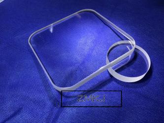
customized thickness Sapphire substrate , , sapphire lens by customized shape,
Sapphire optical window films and substrates with hole,step; gems square sheets and rectangular pieces;
Sapphire lens, sapphire prism, blue / ruby ball, sapphire rod, sapphire laser rod;
Through-hole gem components, precious stones measuring nozzle and inserts, bearings, valve assembly and shaped components and other products;
Production Line:
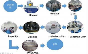
our own factory wuxi fine crystal technology is concerned on production of semiconductor material wafers& optical lens. Main products are the production of large scale integrated2inch,3inch, 4 inches, 5 inches and 6 inches of polished single crystal wafers, Quartz wafers, Sapphire wafers,SiC wafer, GaAs, and a very wide range of custom optics and precision optical components.
With our expanding international network, we can satisfy any customer requirements and be responsive to your exact needs before and after delivery. Our commitment is to consistently provide you with high quality products and services designed to your exact specifications delivered on time at a competitive price.
We are happy to undertake projects of all sizes-from one-off research orders to large scale production runs with call off delivery schedules.
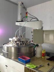
Our team has almost 40persons,and our factory is almost 3000m2,wire-sawcut machine, annealing furnace,surface-grinding machine,orientation device,CNC engraving and milling machine,9B&16B,32B lapped and polished machines,pure water cleaning equipment,contourgraph,surface roughometer etc.
We are happy to undertake projects of all sizes-from one-off research orders to large scale production runs with call off delivery schedules.
It’s our goal to build a lasting relationship with you. It would be great honor to be your friends.
Thank you for considering our company.
R&D:
Our own wuxi factory had taken the national patent certificate about a new method of sapphire processing in 2016.We are working by technology innovation, because science and technology is the first productive force.
Our Team:
Our wuxi fine crystal factory has strong production capacity, we own the domestically top production line and excellent workerswho mainly are researchers and technicians from the Chinese famous semiconductor wafers company .they are experienced and creativity for producing,designing wide range of optical lenses and wafers produce method.
History:
Shanghai famous trade co.,ltd. is established in 2013, and our factory is established in 2014 Wuxi city.Our team is a professional manufacturer and exporter that is concerned with the semiconductor substrates providing ,optical wafer producting .We are located in shanghai with convenient transportation access.All of our products comply with international quality standards and are greatly appreciated in a variety of different markets throughout the world. We have over 30 employees, an annual sales figure that exceeds 150w USD ,and are currently exporting60% of our production worldwide. Our well-equipped facilities and excellent quality control throughout all stagesof production enables us to guarantee total customer satisfaction.
As a result of our high quality products and outstanding customer service, we have gained a global sales network reaching If you are interested in any of our products or would like to discuss a custom order, please feel free to contact us. We are looking forward to forming successful business relationships with new clients around the world in the near future.
Service:
Besides manufacturing optical lens and semi wafers follow customers drawing,we could also supply service of optics design and OEM.
And our after sales service is considerate,you'll feel comfortable to be here;)
Factory Information
Market name:
North America,South America,Western Europe,Eastern Europe,Middle East,Africa,Worldwide