Ecer asks for your consent to use your personal data to:
Personalised advertising and content, advertising and content measurement, audience research and services development
Store and/or access information on a device
Your personal data will be processed and information from your device (cookies, unique identifiers, and other device data) may be stored by, accessed by and shared with 135 TCF vendor(s) and 65 ad partner(s), or used specifically by this site or app.
Some vendors may process your personal data on the basis of legitimate interest, which you can object to by do not consent. Contact our platform customer service, you can also withdraw your consent.
Your message must
be between 20-3,000 characters!
Submit Requirement
Thank You!
Your requirement has been sent. we will contact you quickly!
{"title":"HASL Printed Circuit Board Assembly Services For Electronics Device","imgUrl":"https:\/\/img.chinax.com\/nimg\/3b\/9e\/57a58940e9ddd4ce2ac72028c9ad-200x200-1\/hasl_printed_circuit_board_assembly_services_for_electronics_device.jpg","attrs":{"Brand Name":"CUSTOM MADE","Certification":"ISO\/UL","Place of Origin":"China","Minimum Order Quantity":"Negotiable"}}
{"title":"FR4 RCC PTFE Circuit Board Assembly Environmentally Friendly Solution","imgUrl":"https:\/\/img.chinax.com\/nimg\/86\/74\/22c37f1e7f3f301f54c6d2c0c736-200x200-1\/fr4_rcc_ptfe_circuit_board_assembly_environmentally_friendly_solution.jpg","attrs":{"Brand Name":"CUSTOM MADE","Certification":"ISO\/UL","Place of Origin":"China","Minimum Order Quantity":"Negotiable"}}
{"title":"Automotive Electronics PCB Production With Immersion Gold OSP","imgUrl":"https:\/\/img.chinax.com\/nimg\/15\/24\/7b0f649171735729d4dfd25dbba6-200x200-1\/automotive_electronics_pcb_production_with_immersion_gold_osp.jpg","attrs":{"Brand Name":"CUSTOM MADE","Certification":"ISO\/UL","Place of Origin":"China","Minimum Order Quantity":"Negotiable"}}
{"title":"High Frequency Electronic Component Sourcing PCB Manufacturing Service HASL","imgUrl":"https:\/\/img.chinax.com\/nimg\/2e\/73\/0e189ba1e635071bcffee1154621-200x200-1\/high_frequency_electronic_component_sourcing_pcb_manufacturing_service_hasl.jpg","attrs":{"Place of Origin":"China","Minimum Order Quantity":"Negotiable","Price":"Negotiable","Supply Ability":"100000pc\/Month"}}
{"title":"Custom Printed Circuit Board Fabrication Glue Free Calendered Copper","imgUrl":"https:\/\/img.chinax.com\/nimg\/33\/aa\/151b98b626c73446e3f26b3f2b0e-200x200-1\/custom_printed_circuit_board_fabrication_glue_free_calendered_copper.jpg","attrs":{"Brand Name":"CUSTOM MADE","Certification":"ISO\/UL","Place of Origin":"China","Minimum Order Quantity":"Negotiable"}}
{"title":"Carbon Ink Printed Circuit Board Fabrication Rogers Turnkey Pcb Electronics","imgUrl":"https:\/\/img.chinax.com\/nimg\/36\/a5\/c520471974021a376417b9c3724d-200x200-1\/carbon_ink_printed_circuit_board_fabrication_rogers_turnkey_pcb_electronics.jpg","attrs":{"Place of Origin":"China","Minimum Order Quantity":"Negotiable","Price":"Negotiable","Payment Terms":"T\/T"}}
{"title":"FR4 One Stop PCB Assembly FPC Board Manufacturing Services","imgUrl":"https:\/\/img.chinax.com\/nimg\/fc\/1e\/3c7f138f08573a6e172736c29cd8-200x200-1\/fr4_one_stop_pcb_assembly_fpc_board_manufacturing_services.jpg","attrs":{"Brand Name":"CUSTOM MADE","Certification":"ISO\/UL","Place of Origin":"China","Minimum Order Quantity":"Negotiable"}}
{"title":"2L 64L PCB Assembly Manufacturer Elevate Aerospace Industry Performance","imgUrl":"https:\/\/img.chinax.com\/nimg\/f2\/24\/dccdc05acddab10e156063492b78-200x200-1\/2l_64l_pcb_assembly_manufacturer_elevate_aerospace_industry_performance.jpg","attrs":{"Brand Name":"CUSTOM MADE","Certification":"ISO\/UL","Place of Origin":"China","Minimum Order Quantity":"Negotiable"}}
{"title":"0.04mm SMT PCB Prototype Service High Tg FR4 Multilayer Flexible Pcb","imgUrl":"https:\/\/img.chinax.com\/nimg\/12\/62\/76dce83151850182a0329afcdb8c-200x200-1\/0_04mm_smt_pcb_prototype_service_high_tg_fr4_multilayer_flexible_pcb.jpg","attrs":{"Place of Origin":"China","Minimum Order Quantity":"Negotiable","Price":"Negotiable","Payment Terms":"T\/T"}}
{"title":"Conformal Coating Printed Circuit Board Design Rogers PCB Electronic Board Design","imgUrl":"https:\/\/img.chinax.com\/nimg\/3d\/e3\/9fce07046705ac389afee8a6e6f2-200x200-1\/conformal_coating_printed_circuit_board_design_rogers_pcb_electronic_board_design.jpg","attrs":{"Place of Origin":"China","Minimum Order Quantity":"Negotiable","Price":"Negotiable","Payment Terms":"T\/T"}}
{"title":"Metal Substrate High Speed Pcb Design PTFE Producibility Board Layout Design","imgUrl":"https:\/\/img.chinax.com\/nimg\/09\/96\/d903cab7f75d8b5e7aa85fb3db0a-200x200-1\/metal_substrate_high_speed_pcb_design_ptfe_producibility_board_layout_design.jpg","attrs":{"Place of Origin":"China","Minimum Order Quantity":"Negotiable","Price":"Negotiable","Payment Terms":"T\/T"}}
{"title":"Carbon Ink Pcb Board Design Flexible Multilayer Pcb Design For Electronics","imgUrl":"https:\/\/img.chinax.com\/nimg\/5a\/ed\/83de3995c33ef08de443edc5c6e3-200x200-1\/carbon_ink_pcb_board_design_flexible_multilayer_pcb_design_for_electronics.jpg","attrs":{"Place of Origin":"China","Minimum Order Quantity":"Negotiable","Price":"Negotiable","Payment Terms":"T\/T"}}
{"title":"Mercedes Benz Airbag Reset Tools with Crash Data Stored","imgUrl":"","attrs":{"Place of Origin":"China","Brand Name":"Aototech","Model Number":"AG05","Certification":"CE"}}
Established in 2011 and located in Shenzhen, Guangdong Province, Tongzhan Industrial Ltd. is committed to becoming a leading one-stop Electronic Manufacturing Service (EMS) provider.
We provide customers with top-quality PCB series products. Our services span across PCB design, manufacturing, component procurement, to PCBA design and board making, including supply chain services, functional testing, conformal painting, complete assembly, and more.
Our corporate culture prioritizes serving customers and always putting their needs first.
At Tongzhan, we value diligence and innovation, honesty, and transparency. We are committed to delivering professional, efficient services to achieve win-win results.
Our employees are passionate about science and technology.
Basic Information
Company Name:
TONGZHAN INDUSTRIAL LIMITED
Business Type:
Manufacturer
Employee Number:
50~100
Year Established:
2011
Total Sales Annual:
5000000-10000000
Company Location:
Room 1803, Middle Block,Fujing Building, Fuzhong Road, Futian district, Shenzhen China 518016 New website: https://www.tongzhanpcba.com/
Trade & Market
Company slogan:
TONGZHAN INDUSTRIAL LIMITED
OEM Overview:
PCB customization process
1. PCB custom drawing
2. PCB processing
3. PCB sample proofing
4. PCB board
5. PCB Inspection
6. PCB sample
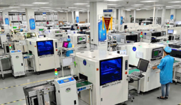
Production Line:
PCB Board Production Process 1. Printed circuit board.
That is, the printed circuit board is printed out with transfer paper. The caveat here is that the slippery side should be facing you. Usually, two boards are printed on one sheet of paper, and the one with the best print is used to make the board.
2. CCL cutting
What is CCL? It is a circuit board with copper film on both sides. Cut the copper-clad laminate and use the photosensitive board to make the full picture of the circuit board. Cut the CCL to the size of the circuit board, being careful not to cut too large and waste material.
3. Pretreatment of CCL
The oxide layer on the surface of the copper-clad laminate needs to be polished with fine sandpaper to ensure that the toner on the thermal transfer paper can be firmly printed on the copper-clad laminate when transferring the circuit board. (Brightly polished, no obvious stains).
4. The adapter circuit board
Cut the printed circuit board into a suitable size, stick the side printed with the printed circuit board on the copper-clad plate, and put the copper-clad plate into the heat transfer machine after alignment to ensure that the transfer paper is not dislocated. Generally 2-3 times transfer, the circuit board can be firmly transferred on the copper-clad laminate.
Tips: The heat transfer machine needs to be preheated in advance, and the temperature is set at 160-200 degrees Celsius. Because the temperature is very high, pay attention to safety when operating!
5. Corrosion circuit boards and reflow soldering machines
First, you need to check that the transfer of the board is complete. If you find that there are several places that are not adjusted properly, you can use a black oil-based pen to repair, and then corrode. When the exposed copper film on the circuit board is completely corroded, the circuit board is removed from the etching solution and cleaned, so that the circuit board can be etched.
The composition of the corrosion solution: concentrated hydrochloric acid: concentrated hydrogen peroxide: water = 1:2:3. When preparing a corrosive solution, drain the water first, then add concentrated hydrochloric acid and concentrated hydrogen peroxide. If concentrated hydrochloric acid, concentrated hydrogen peroxide or corrosive solution is accidentally splashed on the skin or clothes during operation, rinse it off with clean water in time. Due to the use of a strong corrosive solution, be sure to pay attention to safety during the operation!
6. Circuit board drilling
The circuit board needs to insert electronic components, so drilling holes in the circuit board is essential. The choice of drill pin is determined according to the pin thickness of electronic components. When operating the rig for drilling, be sure to stabilize the circuit board and keep the rig speed, not too slow.
7. Circuit board preprocessing
After the previous step (drilling) is completed, the circuit board needs to be pretreated, and the toner covering the board should be polished off with fine sandpaper, and then the circuit board should be cleaned with clean water. After the water on the circuit board is dry, apply rosin to the side with the circuit. The circuit board can be heated with a hot air blower to speed up the solidification of the rosin. It only takes 2-3 minutes for the rosin to solidify.
8. Soldering Electronic Components
This is the final step, soldering all the electronic components to the board and turning on the power. So far, the production process of the PCB board has been completed. Author: CITIC China PCB.
R&D:
PCB Design Process: 1. Preliminary Preparation
Including preparation of component library and schematic diagram. Before designing the PCB, first prepare the schematic SCH component library and the PCB component package library. PCB component footprint libraries are best built by engineers from standard-size data for selected devices. In principle, the component package library of PC is established first, and then the schematic SCH component library is established. The PCB component package library has high requirements, which directly affects the PCB installation; the schematic diagram SCH component library has relatively loose requirements, but pay attention to defining pin attributes and the corresponding relationship with the PCB component package library.
2. PCB Structure Design
According to the determined circuit board size and various mechanical positioning, draw the PCB board frame in the PCB design environment, and place the required connectors, buttons/switches, screw holes, assembly holes, etc. according to the positioning requirements. Consider and determine routed and non-routed areas (for example, how much area around screw holes is non-routed).
3. PCB Layout Design
Layout design is to place the device in the PCB frame according to the design requirements. Generate a netlist in the schematic tool (Design→Create Netlist), and then import the netlist into the PCB software (Design→Import Netlist). After the network table is imported successfully, it will exist in the software background. All devices can be called out via the Placement operation, with flying leads between pins to indicate connections. At this time, the layout design of the device can be carried out. PCB layout design is the first important process in the entire PCB design process. The more complex the PCB board, the more the quality of the layout can directly affect the difficulty of the later wiring. Layout design relies on the basic circuit skills and rich design experience of circuit board designers and is a higher-level requirement for circuit board designers. Junior circuit board designers have little experience and are suitable for small module layout design or PCB layout design tasks with less difficulty in the entire board.
4. PCB Wiring Design
PCB layout design is the process with the largest workload in the entire PCB design, which directly affects the performance of the PCB board. In the process of PCB design, wiring generally has three realms: one is wiring, which is the most basic entry requirement for PCB design; the other is the satisfaction of electrical performance, which is a standard for measuring whether a PCB board is qualified. After connecting, carefully adjust the wiring for optimal electrical performance; again, the wiring is neat and beautiful, and the wiring is messy. Even if the electrical performance test is passed, it will bring great inconvenience to the later board modification, optimization, testing and maintenance, and the wiring requirements are neat. Unity, not criss-cross.
5. Routing Optimization And Silkscreen Layout
"PCB design is not the best, only better", "PCB design is a flawed art", this is mainly because PCB design needs to meet the design requirements of all aspects of hardware, individual requirements may conflict, and fish and fish can 'Both. For example, a PCB design project needs to be evaluated as a 6-layer board by a circuit board designer, but the product hardware must be designed as a 4-layer board due to cost considerations, so the signal shielding ground layer can only be sacrificed, resulting in adjacent wiring. Signal crosstalk between layers increases and signal quality degrades. A general design rule is that optimizing routing takes twice as long as initial routing. After the PCB layout optimization is completed, post-processing is required. The first thing to deal with is the silkscreened logo on the surface of the PCB. When designing, the bottom silkscreen characters need to be mirrored to avoid confusion with the top silkscreen.
6. Network DRC Check And Structure Check
Quality control is an important part of the PCB design process. General quality control methods include design self-inspection, design mutual inspection, expert review meeting, special inspection, etc. Schematic diagrams and structural component diagrams are the most basic design requirements. The network DRC check and the structural check are to confirm that the PCB design satisfies the two input conditions of the principle netlist and the structural component diagram, respectively. Generally, circuit board designers will have their own accumulated design quality checklists, some of which come from a company or department specifications, and the others from their own experience. Special inspections include designed Valor inspections and DFM inspections. These two parts focus on the back-end processing of the PCB design and the processing of the photo painting files.
7. PCB Board
Before the PCB is officially processed and produced, the circuit board designer needs to communicate with the PE of the PCB A board supplier to answer the manufacturer's confirmation questions about the PCB board processing. This includes but is not limited to: the selection of PCB board type, adjustment of line width and spacing of circuit layers, adjustment of impedance control, adjustment of PCB stack thickness, surface treatment process, aperture tolerance control and delivery standards, etc.
Our Team:
Tongzhan was established in 2011 and has an experienced team, most of whom have more than 4 years of experience in PCB design, manufacturing, assembly, and parts procurement. Company B consists of the business department, technology department, production department, quality department and so on. Our people love science, we love technology, and we're all passionate about building a world-renowned company.
Business Department
Technology Department
Production Department
Quality Department
History:
China Tongzhan Industrial Co., Ltd. was established in Shenzhen, Guangdong in 2011.
In 2012, Tongzhan focused on PCB design, manufacturing, assembly, parts procurement, etc.
In 2015, the same exhibition recruited engineers with many years of PCB design and manufacturing experience.
In 2020, Tongzhan will enter the European and American markets and will be widely recognized by customers for its high-quality products and services.
In 2022, Tongzhan is committed to becoming a leading one-stop EMS service provider.
Service:
Tongzhan specializes in providing electronic manufacturing services to customers, our services include PCB design, PCB manufacturing, parts procurement, PCB assembly, and testing. We manufacture using customer-commissioned materials, as well as complete turnkey programs that source, inspect and support raw materials.
We have various assembly services such as PCB and SMT assembly one-stop service, express turnkey PCB assembly, one-stop turnkey PCB assembly, and SMT turnkey PCB assembly.
Tongzhan always pays attention to customer needs, is customer-oriented, and satisfying customer needs is the premise of our survival. By establishing a management system centered on customer service, increasing investment in technology development, improving the quality of employees through internal construction, and meeting all the requirements of customers.
Factory Information
Market name:
North America,South America,Eastern Asia,Southeast Asia